
An optical module aluminum housing is not just a small milled box. In telecom equipment, the housing may support EMI shielding, grounding, heat transfer, connector alignment and clean assembly at the same time.
The hard part is that these requirements often conflict. The part needs to be light and compact, but the shielding contact surface must remain stable. Thin walls reduce weight, but they are easier to distort. Anodizing improves appearance and corrosion resistance, but it can change dimensions and reduce conductivity where electrical contact is required.
For buyers, the key question is not only whether a supplier can machine the shape. It is whether the supplier can separate shielding faces, thermal faces, locating holes, thin-wall areas and surface-treatment masks into a controlled CNC and inspection plan.
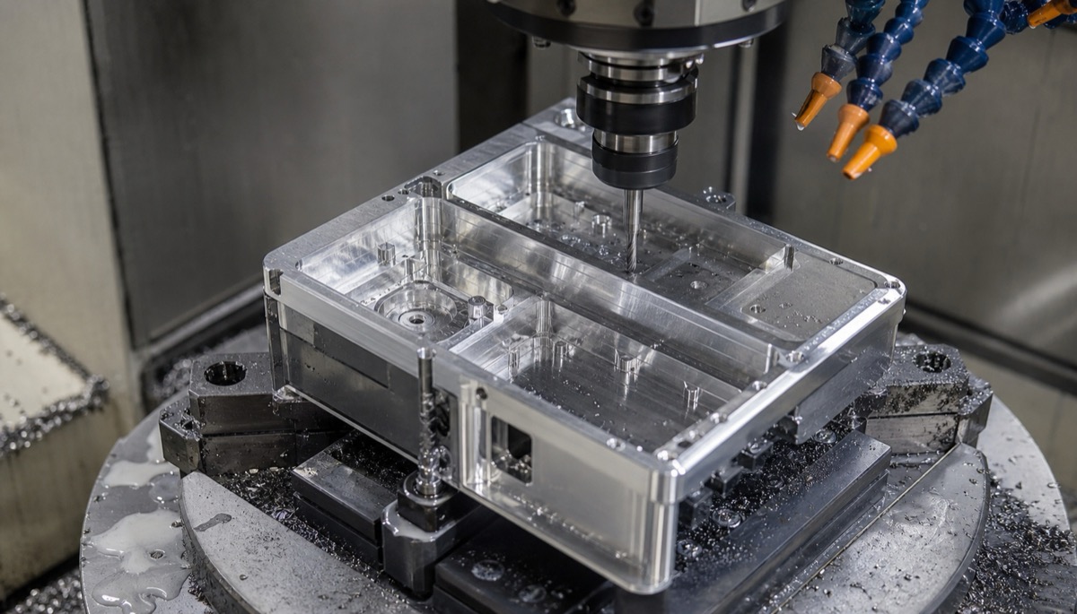
Which Features Matter Most
Optical module housings are usually small, but functional features are dense. A minor error on a shielding step, screw boss or datum hole may cause more trouble than a visible outside dimension error.
| Feature | What to control | Why it matters |
|---|---|---|
| Shielding contact surface | Flatness, tool marks, burrs, masking or post-finish conductivity | Maintains stable EMI shielding and grounding contact |
| Heat-transfer face | Flatness, parallelism, surface finish and cleanliness | Improves contact with thermal pads, lids or heat sinks |
| Thin-wall cavity | Wall thickness, stress release and clamping support | Reduces deformation, vibration and assembly mismatch |
| Connector opening | Position, edge quality and corner radius | Keeps optical/electrical interface aligned |
| Threaded and locating holes | Hole position, perpendicularity and burr control | Prevents assembly tightness and screw damage |
| Anodized or conductive areas | Coating thickness, masking line and final dimension | Prevents coating from changing fit or electrical contact |
How to Machine the Shielding Cavity More Reliably
For shielding cavities, a bright surface is not the main goal. The useful goal is a repeatable conductive contact surface with controlled burrs, edge breaks and coating strategy. If a local area must stay conductive, the drawing should define whether it will be masked before anodizing, machined after anodizing or treated with another conductive finish.
A stable process often starts with rough machining, stress relief if needed, semi-finishing of cavities, final machining of contact faces and a controlled deburring step. On small thin-wall housings, clamping pressure and toolpath sequence can change the final shape as much as the cutter itself.
| Process point | Recommended control | Buyer benefit |
|---|---|---|
| Blank preparation | Confirm material grade, grain direction and machining allowance | Reduces hidden distortion risk |
| Rough machining | Leave even finishing allowance around cavity walls | Avoids pulling one side of the housing |
| Functional faces | Finish shielding and thermal faces after main stress is released | Keeps contact surfaces stable |
| Deburring | Use controlled edge break near contact and connector zones | Prevents burrs without damaging contact length |
| Anodizing plan | Define masking, plug protection, hanger marks and film thickness | Protects final dimensions and conductivity |
| Clean packaging | Control chips, oil, stains and surface scratches | Improves module assembly reliability |
What the Inspection Report Should Show
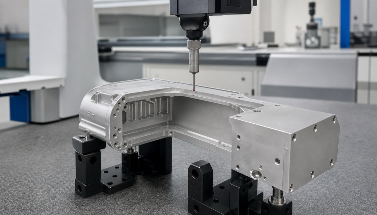
For telecom aluminum housings, a report that only says outside dimensions are within tolerance is not enough. Buyers should check the features that directly affect shielding, heat transfer and assembly. Critical dimensions can be graded, for example from tight functional dimensions such as ±0.005 mm to general enclosure dimensions such as ±0.02 mm or looser, depending on the drawing.
| Inspection item | Buyer focus | Reason |
|---|---|---|
| Shielding step height | Actual value and tolerance from the assembly datum | Controls contact compression and continuity |
| Heat-transfer face flatness | Flatness, parallelism and surface finish requirement | Affects thermal pad contact and heat path |
| Hole position | CMM position report for mounting and locating holes | Prevents module misalignment |
| Thread quality | Go/no-go gauge, depth and entrance burr | Prevents screw seizure or loose assembly |
| Thin-wall deformation | Wall thickness and cavity width after finishing | Confirms the housing did not spring open |
| Post-finish dimensions | Check after anodizing or conductive treatment | Confirms coating did not change the final fit |
How OEMach Handles These Parts
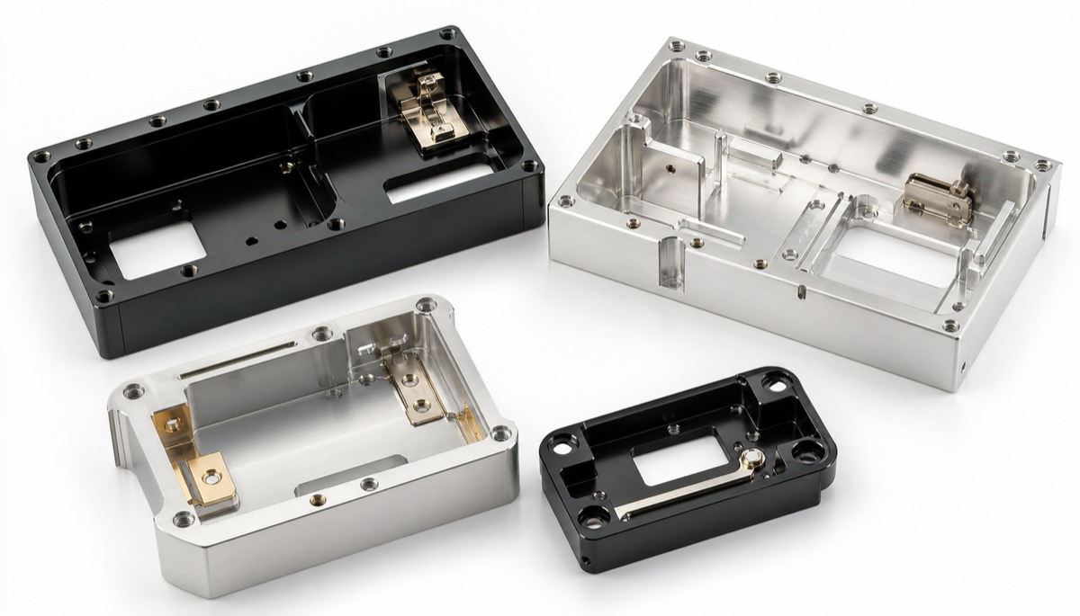
For optical module and telecom aluminum housings, OEMach treats shielding contact faces, thermal faces, locating holes, thin-wall cavities and anodizing requirements as separate risk items during DFM review.
Before machining, the team checks which areas must stay conductive, which faces need flatness control, which holes define assembly position and which features may move after surface treatment. This helps move risk into the first-article stage instead of discovering it during module assembly.
RFQ Checklist for Buyers
| Question to ask | Why it helps |
|---|---|
| Which surfaces are shielding or grounding contact areas? | The supplier can plan masking, finish and burr control |
| Which face is the thermal interface? | Flatness and surface finish can be inspected properly |
| Are any holes datum holes rather than ordinary screw holes? | Position tolerance can be controlled from the right datum |
| What anodizing film thickness and color are required? | Final dimensions and appearance can be planned together |
| Can conductive areas be masked or machined after finish? | Avoids coating blocking electrical contact |
| Do you need CMM data for first articles? | Confirms the process before low-volume production |
FAQ
Why does an optical module housing need shielding-focused machining?
The housing can function as a structural part and an EMI shielding or grounding path. Tool marks, burrs, coating and dents on contact areas can affect electrical contact stability.
Which aluminum alloys are common for optical module housings?
Aluminum 6061 and 7075 are common choices. Selection depends on strength, thermal performance, surface treatment, cost and the required machining stability.
Does anodizing affect shielding contact surfaces?
Yes. Anodized film is usually not ideal for conductive contact. If a local conductive area is needed, masking, film removal or a conductive finishing strategy should be defined before production.
Do these housings need CMM inspection?
Critical holes, shielding steps, thermal faces and thin-wall cavities should be checked by CMM or dedicated gauges when they affect assembly or function.
What files should be sent for quotation?
Send STEP files, 2D drawings with tolerances, surface treatment requirements, conductive area notes, inspection requirements and expected quantity.
Summary
The core of optical module aluminum housing machining is coordinated control of conductive contact surfaces, thin-wall cavity deformation, hole positions, thermal faces, anodizing and cleanliness. Buyers should review these functional details early so the part can be machined, finished and inspected as a reliable telecom enclosure rather than only as a shaped aluminum part.
Ready to get a quote for your CNC machined parts?
Submit your engineering drawings to qiancj@oemach.com. We support prototype sampling and small-batch production with strict tolerance control.